In advanced semiconductor manufacturing, the Electrostatic Chuck (ESC) is a critical component that plays a direct role in wafer yield, process stability, and temperature control.
Its function goes far beyond simply “holding the wafer.” In processes such as plasma etching, thin film deposition, ion implantation, and MOCVD epitaxy, wafers must remain stable under vacuum, high-temperature, and plasma environments. Insufficient wafer clamping can lead to wafer displacement, warpage, and temperature non-uniformity, ultimately affecting process accuracy and production yield.
As a result, electrostatic chucks play multiple critical roles in semiconductor processing, including wafer clamping, temperature control, heat transfer, and overall process stability.
As advanced semiconductor manufacturing continues to move toward higher temperatures, cleaner environments, and tighter process tolerances, conventional ceramic electrostatic chucks are becoming increasingly unable to meet the requirements of high-end semiconductor equipment. In contrast, PBN electrostatic chucks manufactured using CVD technology are emerging as a preferred solution for advanced semiconductor applications.
PBN (Pyrolytic Boron Nitride) is a high-purity ceramic material produced through Chemical Vapor Deposition (CVD) technology.
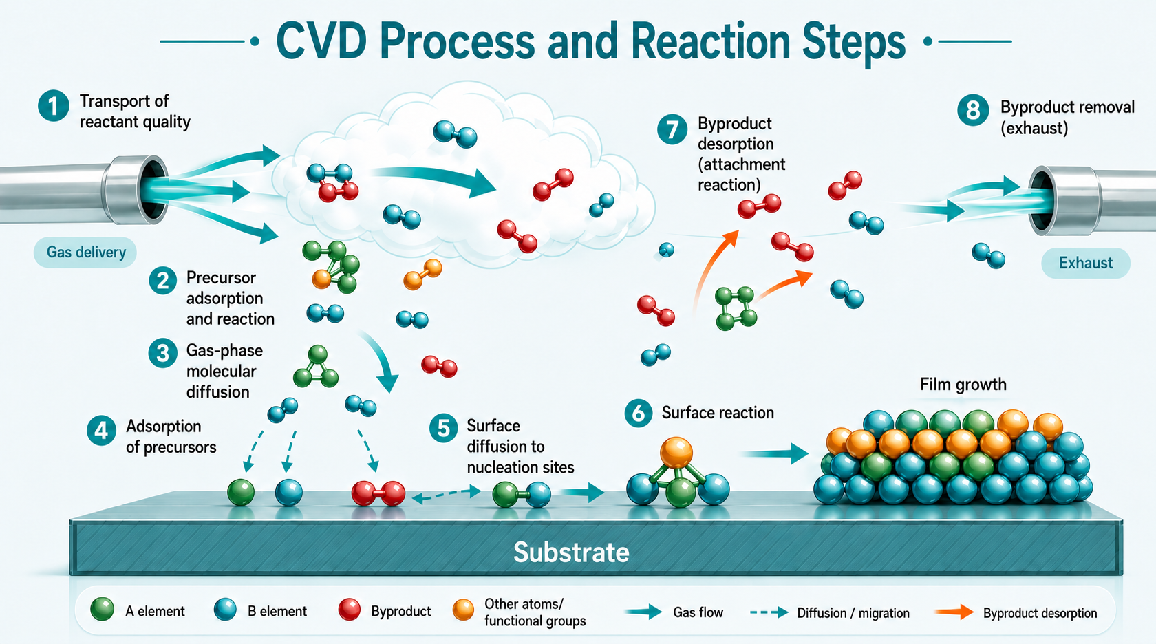
Unlike conventional sintered ceramics, PBN is not produced through powder pressing and sintering. Instead, it is formed layer by layer through a vapor deposition process, resulting in higher purity, a denser structure, and more stable electrical and thermal properties.
The manufacturing process of a PBN electrostatic chuck itself is also a highly precise CVD-based structural fabrication process, designed to meet the stringent performance requirements of advanced semiconductor equipment.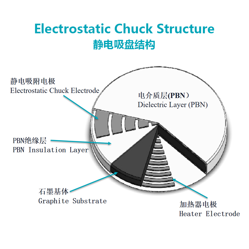
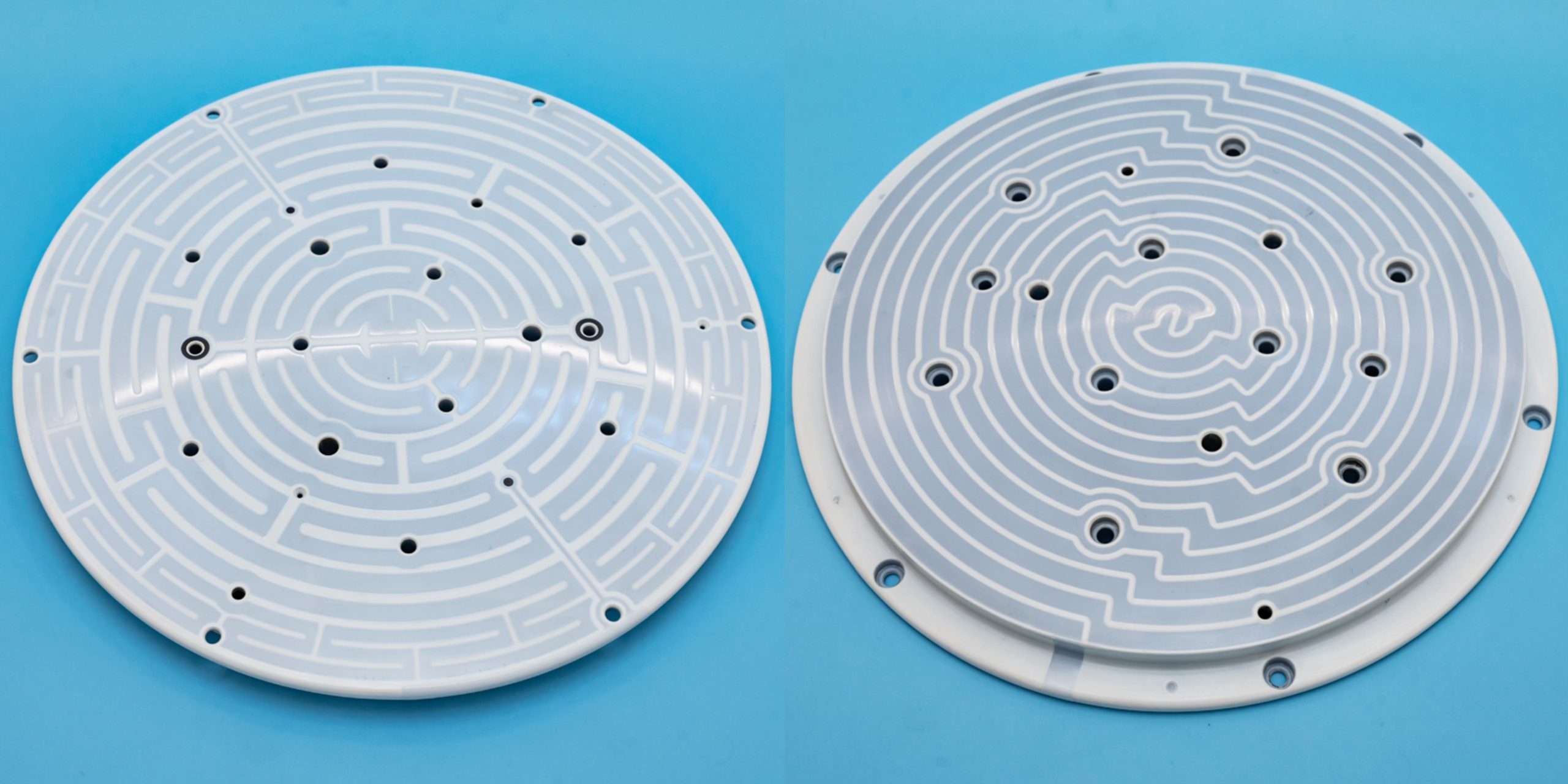
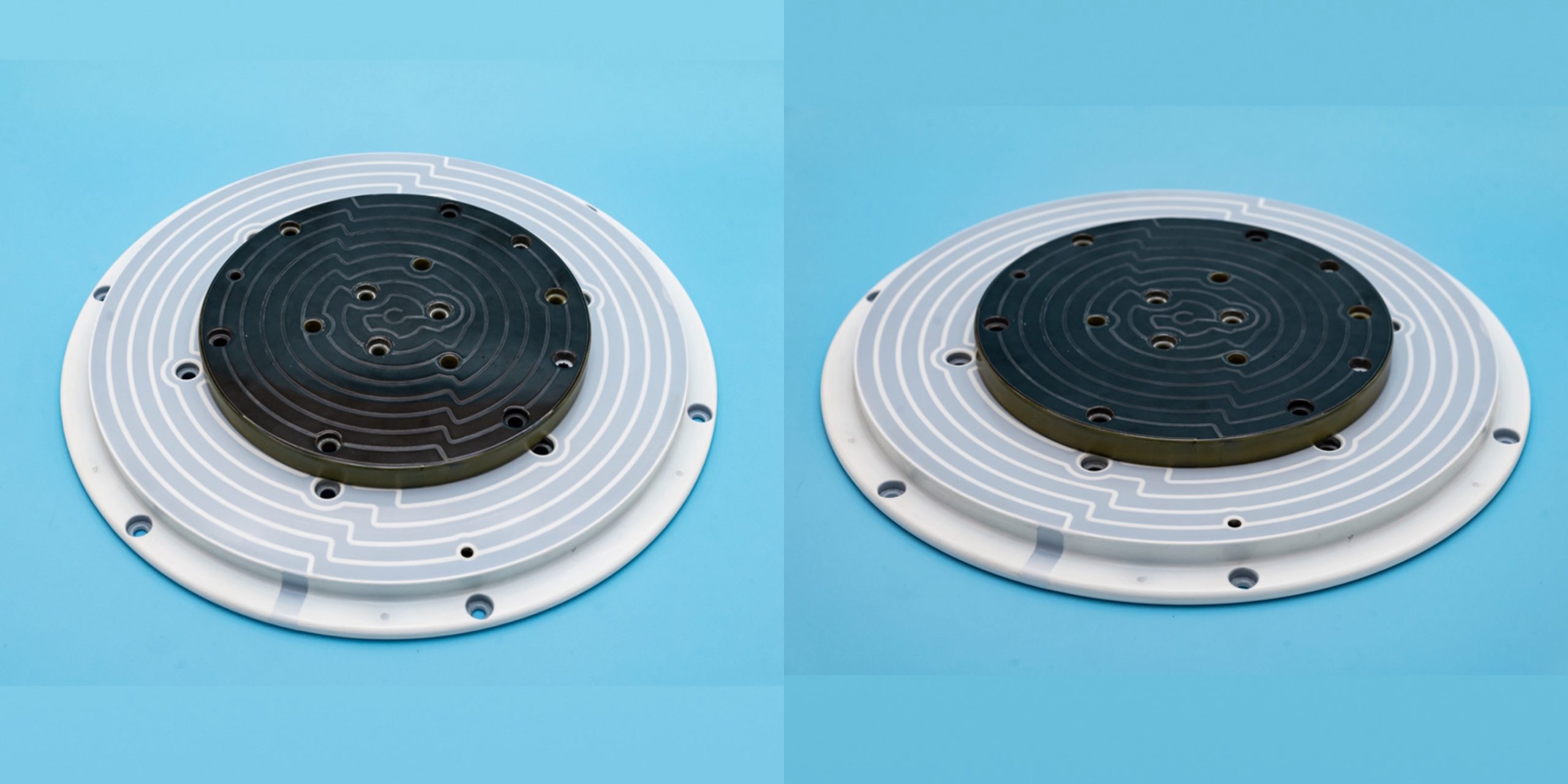
The core structure of a PBN electrostatic chuck is built on a high-purity graphite substrate. A PBN insulating layer is first deposited onto the graphite surface, providing both electrical insulation and a stable foundation for the subsequent functional layers.
Next, a layer of Pyrolytic Graphite (PG) is deposited onto the PBN insulation layer. Due to its excellent electrical and thermal conductivity, PG serves as the functional layer for electrostatic clamping and heating.
Through precision machining processes, the PG layer is then fabricated into internal circuit structures, including electrostatic clamping electrodes and heater electrodes.
Finally, an outer dielectric layer of PBN or C-PBN is deposited through Chemical Vapor Deposition (CVD) technology to form a fully encapsulated structure.
This multi-layer design combines high electrical insulation, high voltage resistance, high-temperature stability, and vacuum cleanliness — key advantages that distinguish PBN electrostatic chucks from conventional ceramic ESCs.
Compared with conventional materials, one of the key advantages of PBN electrostatic chucks is their extremely high purity. The material can reach 5N purity (99.999%), with very low outgassing in high-temperature and vacuum environments, effectively reducing the risk of wafer contamination. This is particularly critical in the semiconductor industry.
As process nodes continue to shrink, even trace levels of contamination inside equipment can significantly affect final device performance. As a result, an increasing number of advanced semiconductor tools are adopting low-outgassing and ultra-clean materials.
In addition to high purity, PBN also offers excellent high-temperature resistance. Unlike conventional ceramic materials, which are prone to thermal stress under elevated temperatures, PBN electrostatic chucks can maintain stable performance during long-term operation in high-temperature environments. This makes them well-suited for high-temperature processes such as MOCVD epitaxy, high-temperature etching, thin film deposition, and third-generation semiconductor manufacturing.
Furthermore, the excellent electrical insulation properties of PBN enable the electrostatic chuck to withstand higher voltages, resulting in more stable electrostatic clamping, reduced leakage risk, and improved wafer holding stability.
For advanced semiconductor equipment, stability is often more important than peak specifications. The key factor affecting yield is not a single performance parameter, but the consistency of long-term process operation.
Today, PBN electrostatic chucks are widely used in semiconductor etching systems, CVD/PVD equipment, MOCVD epitaxial reactors, OLED evaporation systems, and wafer heating and transfer platforms.
As the semiconductor industry continues to move toward higher-end applications, requirements for material performance and process stability will continue to increase. PBN electrostatic chucks manufactured using CVD technology are gradually evolving from a high-end option into a standard critical component in advanced equipment.