Indium Phosphide (InP), a core substrate material for second‑generation compound semiconductors, serves as an irreplaceable key material for DFB and EML lasers as well as APD detector chips. It enables photoelectric conversion in the 1310 nm / 1550 nm communication bands and holds a central position in optical interconnection for computing.
In recent years, the construction of AI computing infrastructure has been accelerating steadily, fueling explosive growth in demand for high‑performance optoelectronic devices. Rapid technological iterations such as 800G / 1.6T / 3.2T high‑speed optical modules and Co‑Packaged Optics (CPO) are driving the optoelectronic material industry including indium phosphide into a new development cycle. Industry analysts forecast that global demand for InP substrates will reach 2.6 million to 3 million pieces in 2026, with the supply‑demand gap exceeding 70%, opening an unprecedented opportunity for the industry.
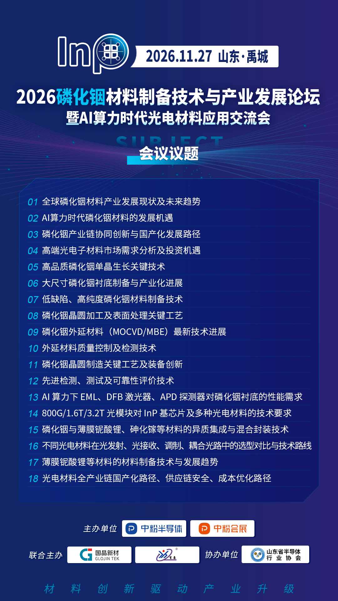
The 2026 Indium Phosphide Material Preparation Technology & Industrial Development Forum and Optoelectronic Materials Application Exchange Conference for the AI Computing Era will be held in Yucheng on November 27, 2026. Glojin Advanced Materials Co., Ltd. will participate in the conference to exchange insights on cutting‑edge technologies and market trends.
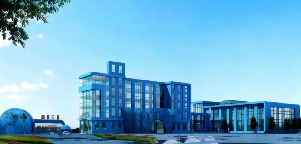
Founded in 2011, Glojin Advanced Materials Co., Ltd. traces its origin back to Shanghai Precision Ceramics established in 2005. It is one of China’s early enterprises engaged in the R&D and production of CVD-series products.
Located in the National High-Tech Industrial Development Zone of Yucheng, Shandong Province, our main offerings include: CVD ceramics (PBN, PG, CVD-SiC, CVD-TaC, etc.), powder ceramics (alumina, aluminum nitride, zirconia, boron nitride, etc.), coating products (PBN coating, PyC coating, TaC coating, SiC coating, B₄C coating, etc.), and semiconductor components (point sources, line sources, electrostatic chucks, ceramic heaters, quartz components, etc.).
Our products are widely adopted in semiconductors, electronic information, artificial intelligence, new energy vehicles, photovoltaics, aerospace, nuclear industry and other sectors. As a leading manufacturer of precision ceramics for China’s semiconductor industry, we serve customers across Japan, South Korea, Singapore, Chinese Taiwan region, Europe and other regions.
Guided by our mission “Drive Innovation, Lead Progress” and core value “Sincerity and Integrity”, we sincerely look forward to cooperating with partners worldwide for mutual benefit and win-win results!
Selected Product Highlights
(1) VGF Crucible

VGF Crucible (Vertical Gradient Freeze Crucible) is a critical vessel for compound single crystal growth via the Vertical Gradient Freeze (VGF) method. It is mainly used to hold molten polycrystalline feedstock. With precisely controlled temperature gradients, the crystal solidifies gradually from the bottom to the top. It is widely applied in semiconductor single crystal growth.
(2) MBE Crucible

MBE Crucible (Molecular Beam Epitaxy Crucible) serves as an effusion cell crucible in molecular beam epitaxy systems to hold evaporant elements and compounds. MBE is a precise thin‑film deposition technique for growing high‑quality single‑crystal thin films. Under ultra‑high vacuum, atomic or molecular beams are directed onto a substrate.
(3) PBN Boat

Pyrolytic Boron Nitride Boat (PBN Evaporation Boat) is a vessel engineered for material holding, thermal treatment and evaporation processes at high temperatures. It delivers long-term stable performance under vacuum or inert atmosphere, is chemically inert to most substances and effectively prevents contamination.

Scan the QR code for more conference information
Conference Organizing Committee
Contact: Mr. Wang
Tel: +86 18263902770 (WeChat available)
Email: wangmeng@cnpowder.com
Note: Images are for non-commercial use. Please notify us for removal if any copyright infringement occurs.