Ultra-high purity (>99.999%) and excellent hermeticity
Excellent electrical insulation
Extremely low outgassing rate at elevated temperatures
Excellent chemical inertness: no reaction with acids, alkalis, salts, or organic solvents at high temperatures
The coating adheres tightly to the substrate and is not easily peeled off
| Performance | Performance | Unit | Value |
| Density | Density | g/cm³ | 1.95-2.20 |
| Tensile Strength | Tensile Strength | N/mm² | 102 |
| Flexural Strength | Flexural Strength | N/mm² | 243 |
| Compressive Strength | Compressive Strength | N/mm² | 244 |
| Thermal Conductivity | (at 200℃) | W/(m·K) | 60 (a-direction); 2.60 (c-direction) |
| Coefficient of Thermal Expansion | (at 200℃) | T.α/(1/K) | 2.0×10⁻⁶ (a-direction) |
| Dielectric Constant (Room Temperature) | Dielectric Constant (Room Temperature) | / | 5.81 |
| Resistivity | Resistivity | Ω·cm | 2.4×10¹⁵ |
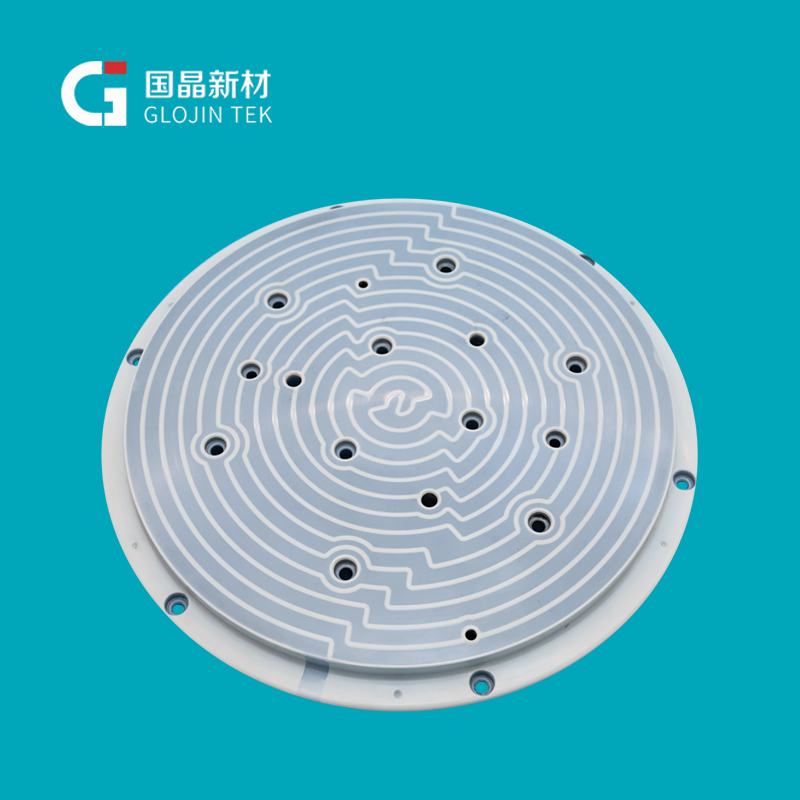
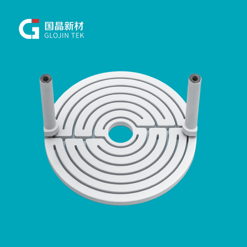
High-temperature heating and insulation components: PBN-coated heaters for wafer annealing processes, etc., featuring excellent heating uniformity and long service life.
No. 88, Nanhuan East Road, Yucheng City, Shandong Province