Conference Background
Indium phosphide (InP), a core substrate material for second-generation compound semiconductors, is an indispensable material for distributed feedback (DFB) lasers, electro-absorption modulated lasers (EMLs), and avalanche photodiode (APD) detector chips. It enables optoelectronic conversion in the 1,310 nm and 1,550 nm telecommunications bands and plays a central role in optical interconnects for AI computing.
In recent years, the rapid expansion of AI computing infrastructure has driven explosive growth in demand for high-performance optoelectronic devices. Technologies such as 800G, 1.6T, and 3.2T high-speed optical transceiver modules and co-packaged optics (CPO) are advancing rapidly, propelling indium phosphide and other optoelectronic materials into a new phase of development. According to industry forecasts, global demand for indium phosphide substrates is expected to reach 2.6–3.0 million wafers in 2026, with the supply shortfall exceeding 70%. The industry is therefore entering an unprecedented window of opportunity.
However, the entire indium phosphide industrial chain still faces several critical challenges. Further breakthroughs are needed in areas including high-quality single-crystal growth, large-diameter substrate preparation, controllability of epitaxial materials, localization of core equipment, improvement of wafer fabrication yields, and advanced packaging technologies. Enhancing material performance, optimizing manufacturing processes, and accelerating domestic substitution have become key priorities for industry-wide collaboration.
Meanwhile, materials such as thin-film lithium niobate and gallium arsenide, which also form part of the technological foundation of the optical communications industry, are facing significant development opportunities as well as technical challenges. A range of optoelectronic materials will advance in parallel and together form the material foundation for optical interconnects in the era of AI computing.
From an industrial-chain perspective, Shandong and its surrounding areas are home to a major cluster of equipment and consumables suppliers serving China’s indium phosphide crystal-growth sector. The region hosts numerous established companies, including Glojin Advanced Materials, a supplier of PBN crystal-growth crucibles, and Yuhao Microelectronics, a manufacturer of crystal-growth furnaces. With the ability to support requirements across the entire process chain, the region has become a key destination for equipment evaluation related to indium phosphide projects.
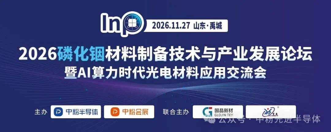
Against this backdrop, China Powder Semiconductor, together with Glojin Advanced Materials and Yuhao Microelectronics, will hold the 2026 Forum on Indium Phosphide Material Preparation Technology and Industrial Development & Conference on Optoelectronic Material Applications in the Era of AI Computing on November 27, 2026.
Under the theme “Driving Industrial Upgrading Through Materials Innovation,” the event will focus on indium phosphide crystal growth, substrate preparation, epitaxial technologies, photonic chip design, device packaging, market applications, and industrial investment. It will also explore technological advances and market prospects for thin-film lithium niobate and other optoelectronic materials.
Representatives from research institutes, leading universities, materials suppliers, epitaxial wafer manufacturers, equipment manufacturers, photonic chip and optical module companies, and end-user organizations will be invited to discuss technological frontiers, industry trends, and opportunities for cooperation. The event aims to support the development of a more complete, efficient, and collaborative materials industry ecosystem.
Organizations and professionals from relevant fields are warmly invited to register and participate.
Date
November 27, 2026
Registration: November 26, 2026
Venue
Conference Hall, Glojin Advanced Materials, Yuwang Group
Yucheng, Shandong, China
Organizers

Co-organizers
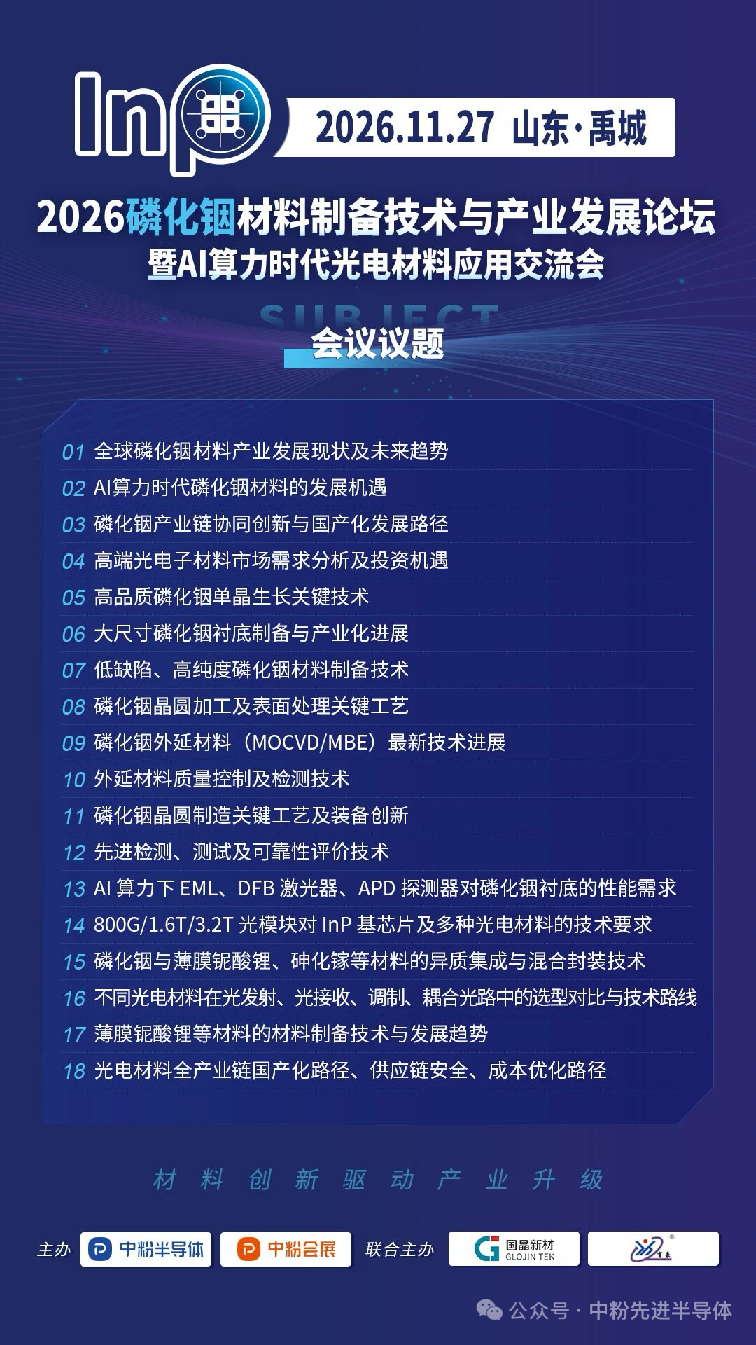
Conference Topics
Part I: Industrial Development
Part II: Materials and Crystal Growth
Part III: Epitaxy and Manufacturing
Part IV: Applications in Photonic Chips and Front-End Devices for Optical Modules
Part V: Coordinated Development of Multiple Materials
Special Activities
The conference will collect information from participating companies concerning technical cooperation, product procurement, process solutions, and other requirements, and organize on-site business matchmaking activities. Relevant information will also be displayed on exhibition boards to improve the efficiency of communication and collaboration during the event.
Topics to be collected include, but are not limited to:
Conference Format
The conference will primarily consist of keynote presentations and on-site discussions. Materials suppliers and equipment manufacturers are also welcome to organize small-scale exhibitions.
To help ensure the success of the conference, companies and research institutions are warmly invited to sponsor the event and enhance their industry visibility through this opportunity.
Registration Fee
RMB 2,800 per person, including conference proceedings and materials, tea breaks, conference meals, and the conference dinner.
Advance Registration Before October 1:
Early-bird rate: RMB 2,300 per person
Group rate for two or more participants: RMB 2,000 per person
Conference Sponsorship
Please contact the conference organizing team for detailed sponsorship information.
Conference Organizing Team
Contact: Mr. Wang
Tel.: +86 182 6390 2770
WeChat: +86 182 6390 2770
Email: wangmeng@cnpowder.com