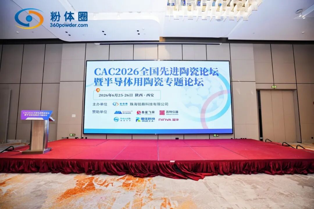
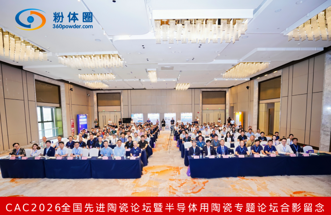
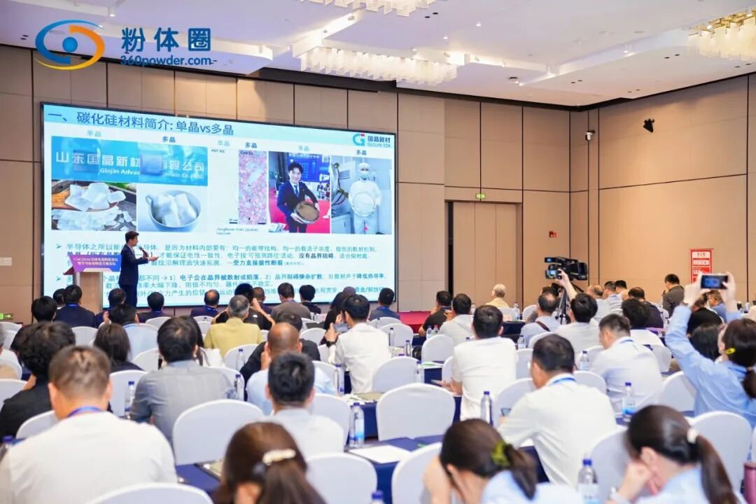
Hosted by Powder Circle, CAC2026 National Advanced Ceramics Forum & Special Forum on Semiconductor Ceramics successfully concluded in Xi’an on June 25–26, 2026.Focusing on technical applications and domestic breakthroughs of advanced ceramics in high-end semiconductor manufacturing, the forum gathered over 200 experts from university research teams and industrial chain enterprises nationwide. Participants conducted systematic discussions on semiconductor precision ceramic materials, manufacturing processes and industrialization challenges, building a professional and efficient exchange platform for the collaborative development of industry, university and research institute in this sector.
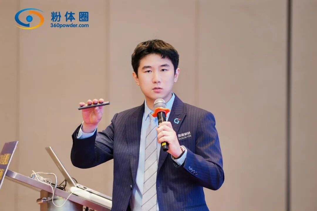
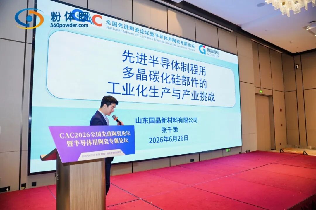
Glojin Advanced Materials Co., Ltd. was invited to attend the forum. Dr. Zhang Qiance, R&D Director of the company, delivered a special report on site, sharing frontline industrialization research achievements and technical insights on the industrialized production and industrial challenges of polycrystalline silicon carbide components for semiconductors.
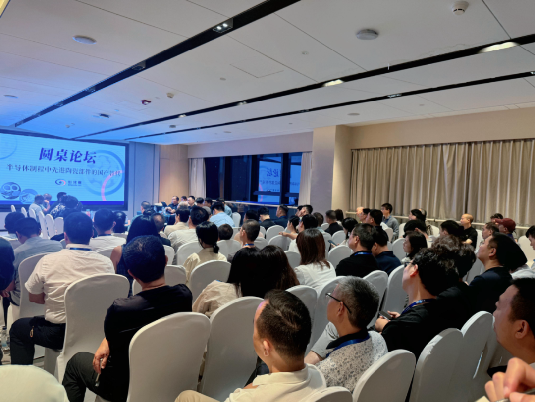
The forum took “domestic substitution of semiconductor ceramics” as its core theme.
During the roundtable discussion on the evening of June 25, industry experts reached a consensus that domestic high-end semiconductor ceramics currently suffer from insufficient powder stability, poor batch consistency, immature precision machining technology and insufficient coordination between upstream and downstream processes. There is still a considerable gap compared with the mature industrial systems of Japan and South Korea. Joint research between industry, universities and research institutions is urgently needed to make up for shortcomings in basic materials and core processes.
The technical report session on June 26 featured rich and comprehensive content. Experts from Tsinghua University, Xi’an Jiaotong University, Shanghai University and leading enterprises in the industry systematically sorted out the current technical status, application difficulties and development trends of advanced semiconductor ceramics from multiple dimensions including semiconductor ceramic substrates, coating technology, precision machining, powder control and structural optimization, providing important references for technological upgrading of the entire industrial chain.
Based on actual semiconductor production scenarios, the report systematically elaborated on issues concerning the industrialization and mass application of polycrystalline silicon carbide components.
The report first summarized the wide applications of polycrystalline silicon carbide in semiconductor equipment, covering core precision components such as MOCVD susceptors, epitaxial bases, wafer boats, etching rings, focus rings and shower heads. It specified the stringent technical standards of advanced manufacturing processes for silicon carbide materials, including high purity, excellent stability, highly uniform temperature field and low impurity precipitation.
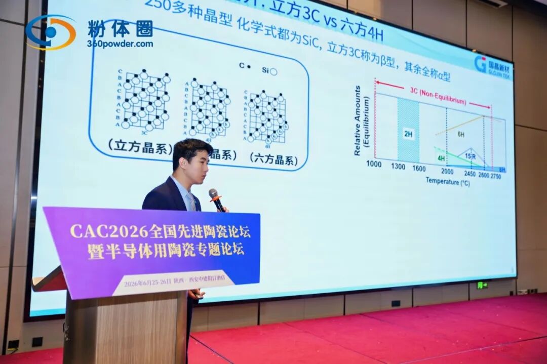
Combined with years of industrialization practice, Dr. Zhang focused on analyzing the common technical bottlenecks faced by the domestic polycrystalline silicon carbide industry, including temperature field control precision of furnaces, graphite substrate compatibility, stability of coating processes and difficulties in precision machining of complex structures.
Meanwhile, the report objectively analyzed the industry deficiencies of domestic polycrystalline silicon carbide components at the present stage in terms of mass production consistency, long-term working stability and systematic process specifications.
Based on the current industrial situation, the report pointed out that the localization of semiconductor silicon carbide ceramics relies not only on breakthroughs in single processes, but also on establishing a full-process systematic management and control system, continuously improving industrial standards and product verification systems. With joint efforts from upstream and downstream partners, the process adaptability and industrial maturity of domestic precision ceramic components will be steadily improved.
The CAC2026 forum has built a high-quality platform for Glojin Advanced Materials Co., Ltd. to exchange technologies and benchmark cutting-edge developments with top domestic research teams and industry peers.
By participating in multi-dimensional technical seminars, the company has gained a clearer understanding of the industry development trend and technical iteration direction of silicon carbide ceramics for semiconductors, accumulating valuable experience for subsequent process optimization, product upgrading and technological innovation.
In the future, Glojin Advanced Materials Co., Ltd. will continue to devote itself to the field of advanced semiconductor ceramics. We focus on the R&D and production of core semiconductor vacuum thermal field materials and components including polycrystalline silicon carbide, pyrolytic boron nitride (PBN) and pyrolytic graphite. The company will continuously refine manufacturing processes, consolidate product quality, and steadily promote the localization process of precision ceramic materials for the semiconductor industry.